Electron Microscopy

  • Momentum resolved STEM

    What we do

    We investigate our samples using high-energy electron beams to obtain images with resolution down to the atom scale. We focus on the development of quantitative methods for electron microscopy.

  • comparison of different inputs

    What we do

    We investigate our samples using high-energy electron beams to obtain images with resolution down to the atom scale. We focus on the development of quantitative methods for electron microscopy.

  • beam electron diffraction patterns

    What we do

    We investigate our samples using high-energy electron beams to obtain images with resolution down to the atom scale. We focus on the development of quantitative methods for electron microscopy.

  • Electrical Polarization

    What we do

    We investigate our samples using high-energy electron beams to obtain images with resolution down to the atom scale. We focus on the development of quantitative methods for electron microscopy.

Electron Microscopy

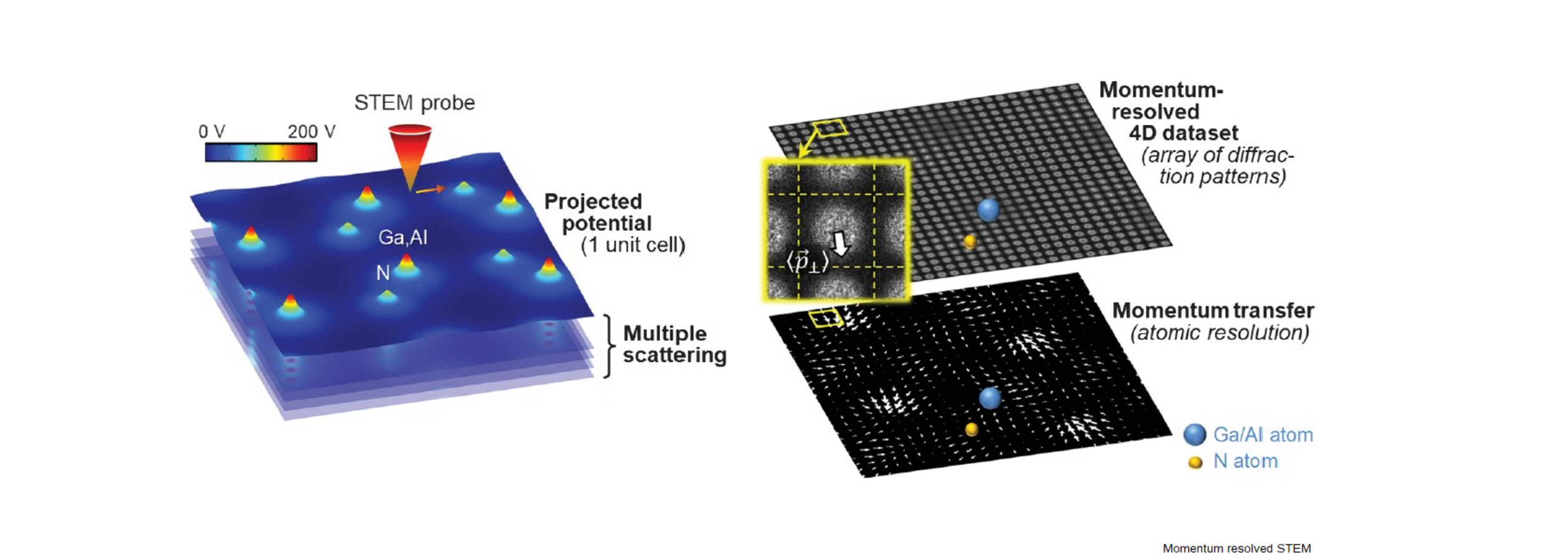
We use transmission electron microscopy (TEM) to investigate the atomic structure and composition of nanomaterials. In the high-resolution TEM (HRTEM) mode the whole region of interest of our specimen is illuminated with the electron beam and the image is formed with the objective lens and further magnifying lenses. In the Scanning TEM (STEM) mode, the electron beam is focused to a diameter down to 50 pm. The focused beam is scanned over the specimen and scattered electrons are detected with different detectors. Images are formed by plotting the detector signal at each scan position.  The composition of the specimen is measured with energy dispersive X-ray analysis (EDX) and energy loss spectroscopy (EELS). Electron tomography yields the 3D structure of our specimen.

What kind of result do I get?

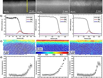
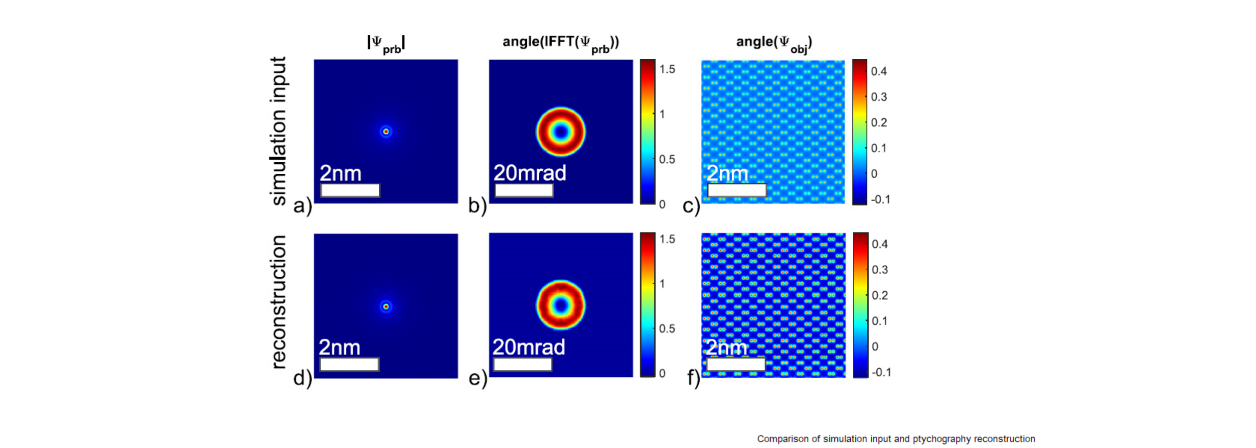
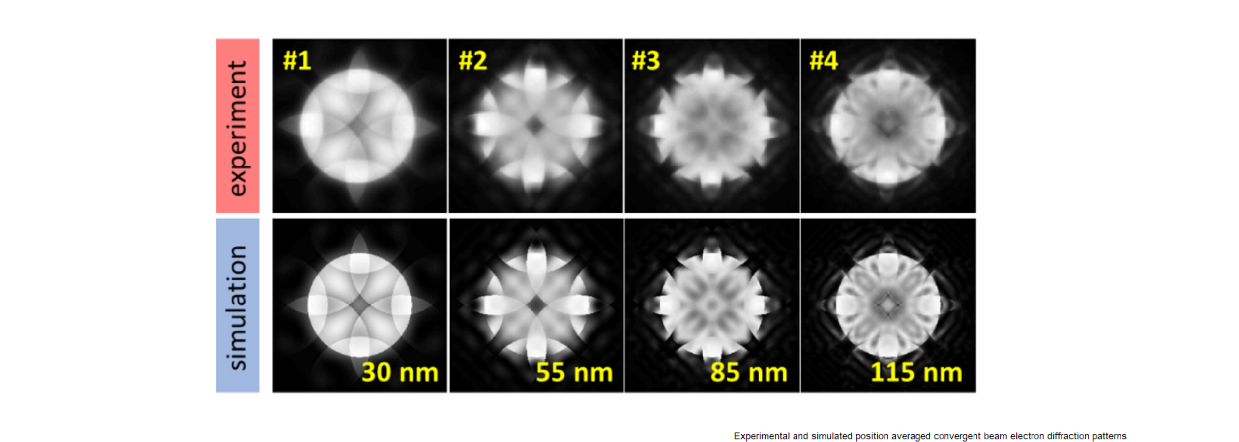
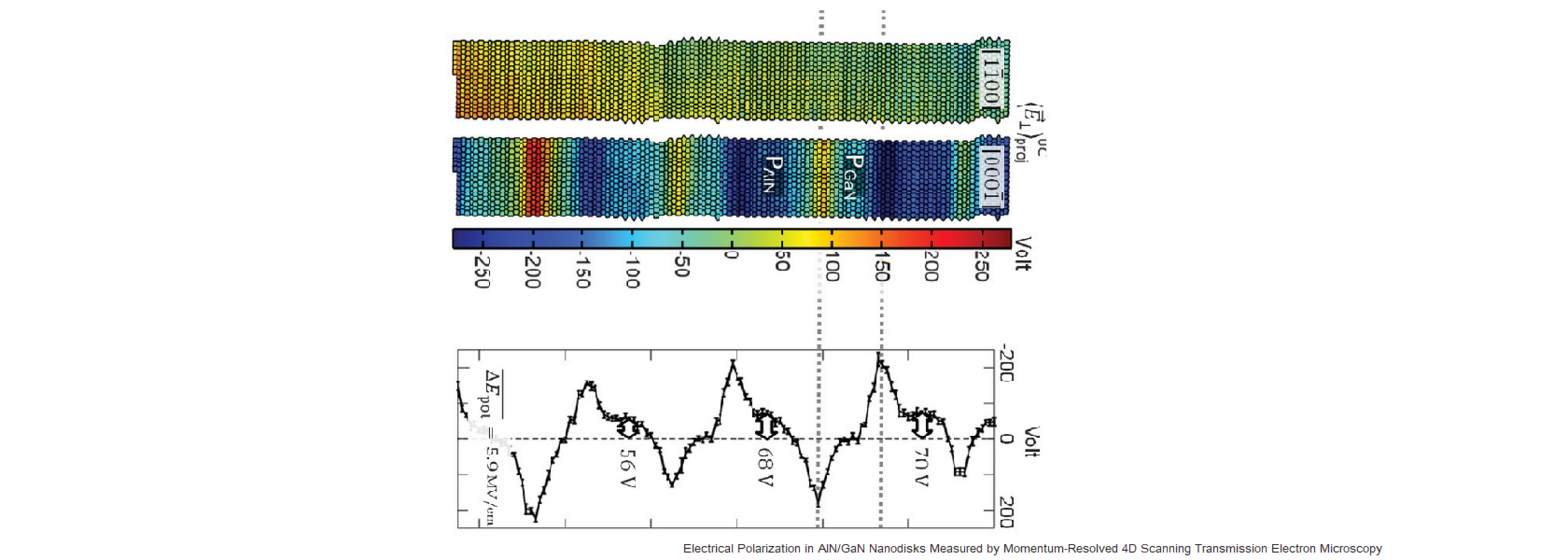
The high-resolution TEM and STEM images show the atomic structure of the specimen projected along the electron beam direction. The images reveal the crystal structure, dislocations and stacking faults. The positions of atom columns are measured with an accuracy of a few picometers. Distances between atom columns give information on the strain distribution in our specimen. In the STEM mode, using the high-angle annular dark field (HAADF) detector, the brightness of an atom column increases with the atomic number, so that we can distinguish different elements in the images. An atom hit by the electron beam emits a characteristic X-ray spectrum. Its measurement in STEM allows 2D elemental mapping, detecting elements even at small concentrations below 1%.

Area responsible

Prof. Dr. rer-nat. Andreas Rosenauer

Service Electron Microscopy

Application Scientist

Dr. Marco Schowalter


MAPEX Center for Materials and Processes
University of Bremen

Otto-Hahn Allee 1, D-28359 Bremen
Phone: +49 421 218 62263
Email: schowalter@ifp.uni-bremen.de


Dr. Thorsten Mehrtens


MAPEX Center for Materials and Processes
University of Bremen

Otto-Hahn Allee 1, D-28359 Bremen
Phone: +49 421 218 62273
Email: mehrtensprotect me ?!ifp.uni-bremenprotect me ?!.de
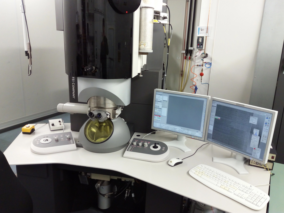
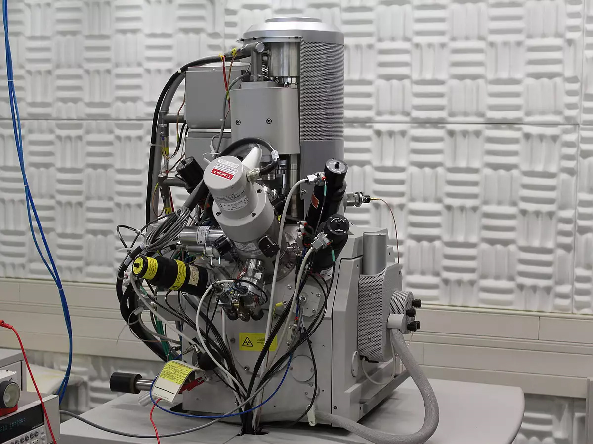
Our key instruments

FEI Titan picture

FEI TITAN 80/300
Image corrected (scanning) transmission electron microscope

  • resolution 80 pm in TEM and 130 pm in STEM
  • EDX, EELS, Möllenstedt-Dücker biprism
  • Tomography holder
mehr
Thermo Fischer picture

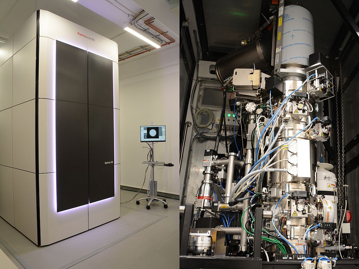
Thermo Fisher  SPECTRA 30/300
Probe corrected (scanning) transmission electron microscope

  • STEM resolution 50 pm
  • X-FEG, Monochromator
  • Electron Microscope Pixelated Array Detector (EMPAD)
    (direct electron detector with 1000 frames per second)
  • Super-X EDS detector
  • On-axis 360° rotation tomography holder
  • dual-axis tomography holder
mehr
electron scanning microscope

FEI Nova 200 NanoLab
Scanning electron microsope with focused Ga-ion Beam

  • Preparation of TEM samples
  • SEM resolution 1-2 nm
  • acceleration voltage 2 kV – 30 kV
  • probe current 2.5 pA – 37 nA
  • Platinum metal deposition

More available instruments

More information about the instrumentation available at MAPEX and MAPEX-CF can be found in the Instrument Database of the MAPEX Center for Materials and Processes.

A click on the logo will lead you to the database.

Research Highlights

Characterization of structure and mixing in nanoparticle hetero-aggregates using convolutional neural networks: 3D-reconstruction versus 2D-projection article picture
Electron Microscopy|

Characterization of structure and mixing in nanoparticle hetero-aggregates using convolutional neural networks: 3D-reconstruction versus 2D-projection

Christoph Mahr, Jakob Stahl, Beeke Gerken, Florian F. Krause, Marco Schowalter, Tim Grieb, Lutz Mädler, Andreas Rosenauer

Ultramicroscopy 265 (2024): 114020

https://doi.org/10.1016/j.ultramic.2024.114020

Structural and chemical characterization of nanomaterials provides important information for…


Composition and strain of the pseudomorphic α-phase intermediate layer at the Ga2O3/Al2O3 interface pic
Electron Microscopy|

Composition and strain of the pseudomorphic α-phase intermediate layer at the Ga₂O₃/Al₂O₃ interface

M. Schowalter, A. Karg, M. Alonso-Orts, J. A. Bich, S. Raghuvansy, M. S. Williams, F. F. Krause, T. Grieb, C. Mahr, T. Mehrtens, P. Vogt, A. RosenauerM. Eickhoff

APL Materials 12 (2024): 091104

https://doi.org/10.1063/5.0226857

We investigate the composition of α-phase intermediate layers at…


Synergizing ICP-MS, STEM-EDXS, and SMPS single particle analytics exemplified by superlattice L10 Pt/Fe aerosol nanoparticles produced by spark ablation article text
Electron Microscopy|

Synergizing ICP-MS, STEM-EDXS, and SMPS single particle analytics exemplified by superlattice L1ₒ Pt/Fe aerosol nanoparticles produced by spark ablation

Vinzent Olszok, Philipp Rembe, Tim Grieb, Eshan J. Wijeyeratnam, Andreas Rosenauer, Alfred P. Weber 

Nanoscale Advances 6(15) 2024: 3895-3903

https://doi.org/10.1039/D4NA00276H

Spark ablation was used to continuously synthesize bimetallic L10 Pt/Fe nanoparticles in an aerosol process involving a…


Aktualisiert von: MAPEX