
© This is an open-access article distributed under the terms of the Creative Commons Attribution (CC-BY) Licence
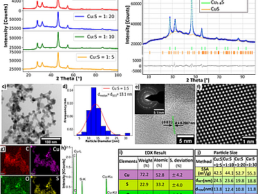
X-Ray Diffraction|
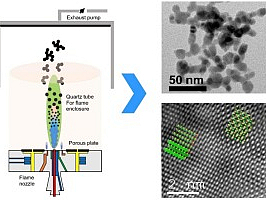
Electron Microscopy|